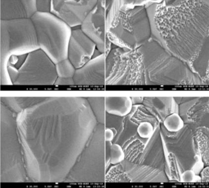
The realization of improved high-performance transistors has become increasingly challenging due to difficult requirements for reduced power dissipation during operation and in stand-by mode, which are necessary to meet Moore’s Law by scaling down Si-based complementary metal-oxide-semiconductor (CMOS) devices. Moreover, increasing operating frequency and higher integration density make the power constraint issue even more challenging. Therefore, researchers have devoted much effort to develop high-performance transistors with high mobility and low operating voltage. The III-V semiconductors such as GaAs, InAs, InGaAs, GaN, InSb, etc. are the potential candidates for high-speed transistors with very low supply voltage. Among them the QWFET with InSb channel materials has a very high mobility than that of others. We have succeed to deposit high-k dielectric on the InSb QW using atomic layer deposition (ALD) technique experimentally. This triumph opens door to realize high-speed and low supply voltage InSb QWFET. We have successfully design and performance high-speed and low consumption voltage InSb QWFET studied by simulation. We are looking forward interested students (M.Sc./ M.Sc. Engr./ M.Phil.) on the III-V compound semiconductor base QWFET design and performance study by simulation.
III-V Quantum Well Field Effect Transistor (QWFET)